At the George Washington University, students don’t just learn about the innovations that will define the national and global future. They also get hands-on experience with cutting-edge technology used by the researchers and industries shaping that future right now.
In Gina Adam’s “Micro and Nanofabrication Techniques” class last semester at the School of Engineering and Applied Science, graduate and undergraduate students became experts in the material techniques by which semiconductor chips—the fundamental technology at the heart of computers, phones, smart devices and much more—are designed, built and refined.
Adam, an associate professor of electrical and computer engineering, uses chips received as part of her partnership with the National Institute of Standards and Technology’s (NIST) Nanotechnology Xcellerator. Students design and build new structures on top of existing fabricated ones, demonstrating for themselves how these structures work and what their interplay can achieve.
After receiving a strong foundation in theory, students in the class get the opportunity to see how that theory applies to the real world—and, of course, how it doesn’t. Extensive engineering was involved in building the GW Nanofabrication and Imaging Center (NIC), where Adam and her students work, so it could host sensitive instruments while mitigating any disturbance from the nearby subway stop, which might otherwise cause building vibrations or interference. The students also went through an extensive process to optimize the actual size at which microstructures can be built and integrated while remaining effective.
“I’m very familiar with the theory of transistors, but I had never done practical exercises,” said Zhiqiang “Ethan” Yi, a second-year master’s student in computer engineering. “There were many things out of my expectation—many surprises in practice.”
“It's been really fun to actually be able to go into the cleanroom and make devices and learn how all the tools work,” said Dylan Roberts, a rising senior majoring in computer engineering. Below, GW Today goes inside one of the final lab sessions of the year. (All photos by Chasity Smith.)

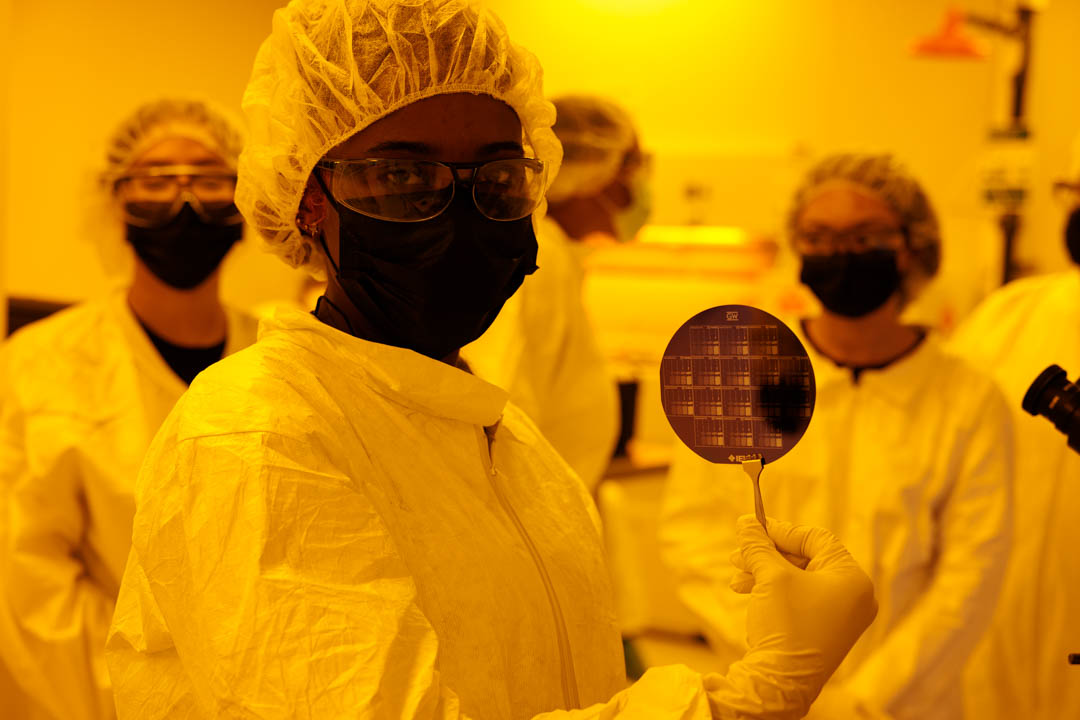
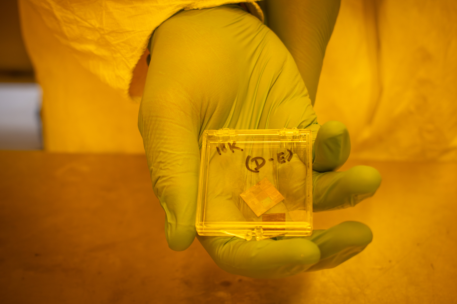
This silicon wafer held by Adam contains 24 different microchip prototypes provided by the Nanotechnology Xcellerator in partnership with NIST, Google, SkyWater and other academic partners. Several were designed by Adam and her team in 2022, and in 2024 the wafers were received and diced for use in research and education. As part of the Micro- and Nanofabrication Techniques class, students worked in teams of two or three, each team assigned a different prototype microchip to use as a starting point for integration.
Most electronic technology is based on integrated circuit technology, which involves transistor devices resembling an infinitesimal layer cake with stacks of interconnections. Each chip is printed with structures directing electricity internally and with vias conducting electricity from one layer of the “cake” to another. New innovations in microelectronics require heterogeneous integration, where new devices have to be fabricated on top of existing chips three-dimensionally to provide increased functionality and better speeds.
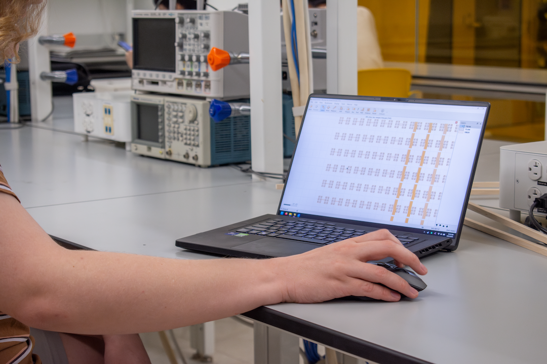
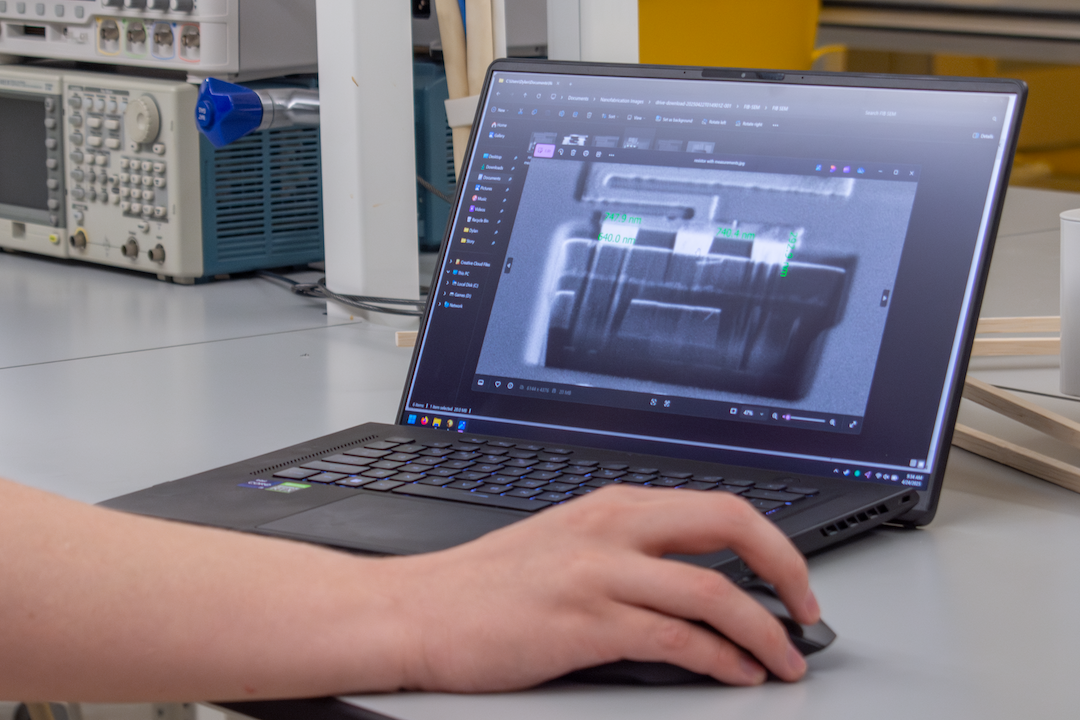
In Adam’s class, students learned the basics of heterogeneous integration by integrating new devices on the existing microchips. First, they used a computer-assisted design (CAD) program to create their own structures aligned to the designs of the existing structures on the microchip (demonstrated above by Dylan Roberts). Then, they learned how to use specialized micro- and nanofabrication tools to make these structures on test wafers and finally integrated on the microchips.
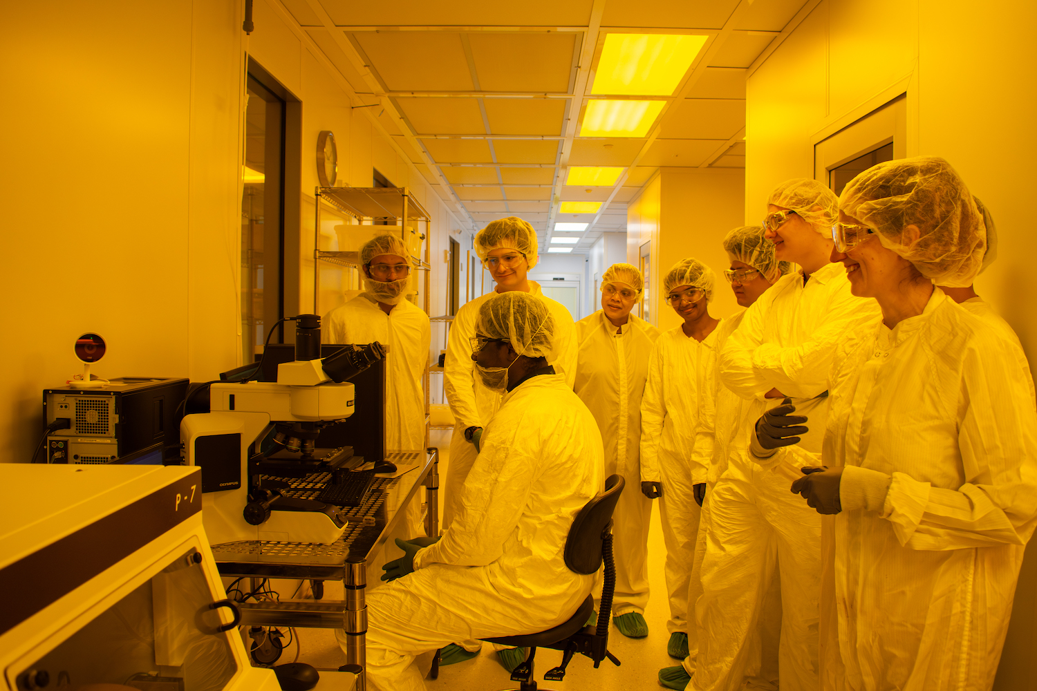
GW NIC is a clean laboratory, meaning anyone entering has to gown up in a special jumpsuit, gloves, overshoes, a bonnet and goggles, plus a mask for those with facial hair, to prevent introducing contaminating particles from the outside.

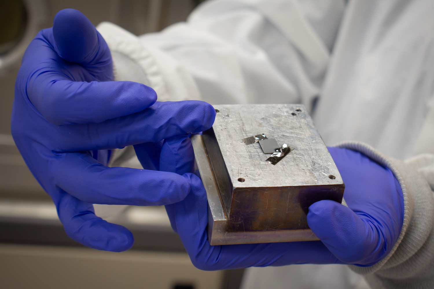
Between fabrication stages, the students carefully use powerful chemicals to clean byproduct deposits and residue off the chips and reveal the optimized structures.
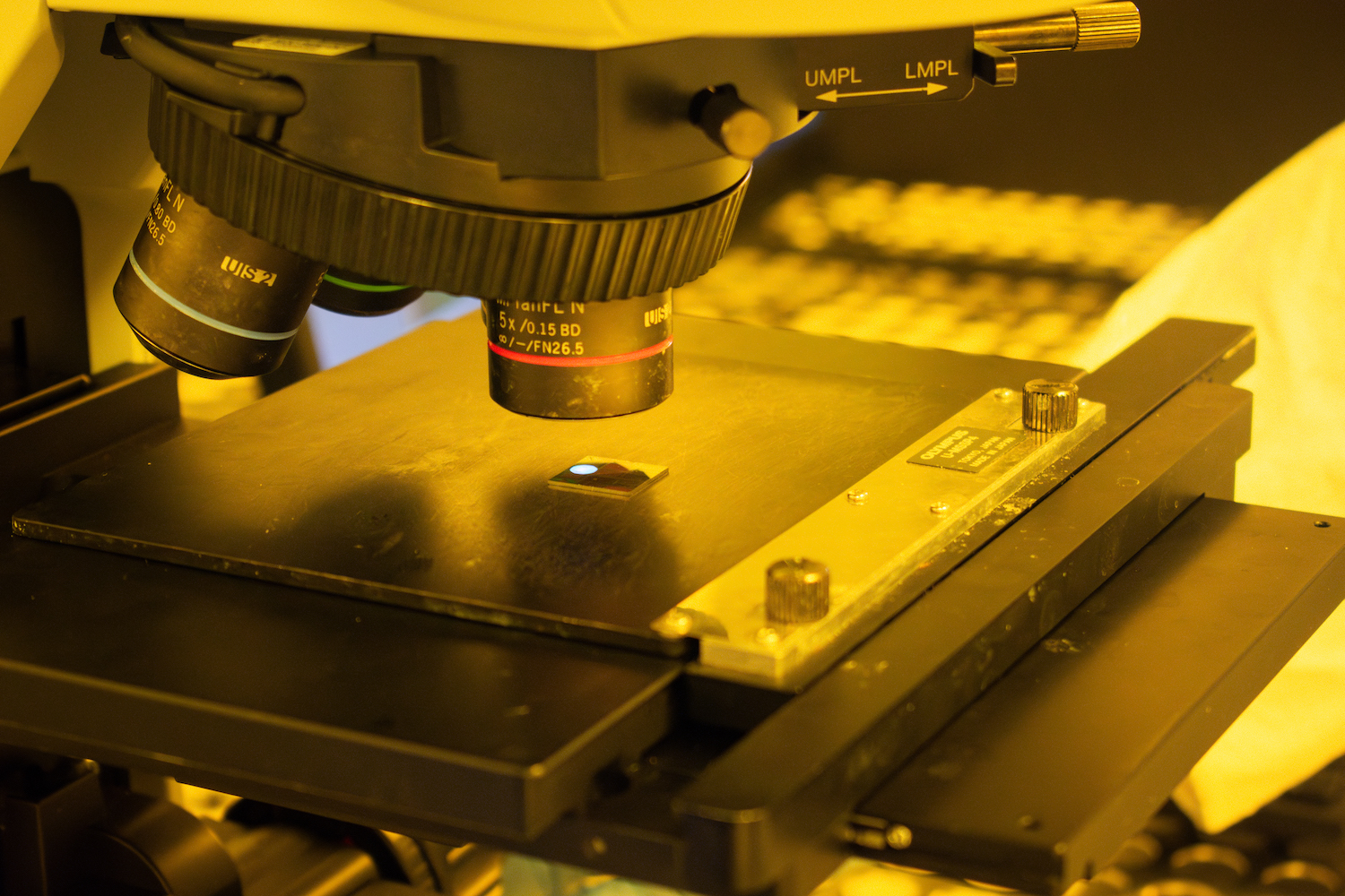
Since each microchip is about the size of a thumbnail, the structures created atop them can only be viewed clearly through a microscope. For the most delicate work, students have the opportunity to use the ultra-powerful focused ion beam scanning electron microscope (FIB-SEM), which can magnify an object at up to 80,000 times its size. Some students said access to an instrument of that caliber was a highlight of the class.
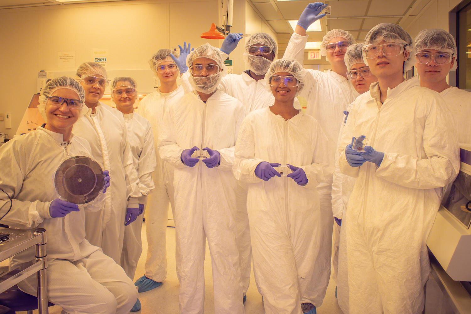
Every student team left the class having integrated their own designs onto a microchip—a powerful qualification in the quickly-evolving semiconductor workforce these GW Revolutionaries will be part of.