Only about 10 to 14 percent of microchips sold globally are manufactured in the United States. Microchips are typically based on transistor devices, and manufacturers cannot risk incorporating new types of devices in production until those devices’ integration feasibility has been demonstrated. Research and development of such demonstrations can be enormously expensive, but the U.S. now aims both to expand its manufacturing presence and to maintain leadership in emerging technologies.
A new collaboration aims to overcome the gap between inventing new devices in the lab and manufacturing new chips in commercial foundries by providing semiconductor microchip prototypes that can be used to demonstrate integration of new devices in the early stages of innovation.
The George Washington University is one of five academic research partners working with the U.S. Department of Commerce's National Institute for Standards and Technology (NIST), Google and semiconductor manufacturer SkyWater Technology to create a domestic, affordable supply of such microchips for researchers and startups. The collaboration aims to unleash innovation in the semiconductor and nanotechnology industries and comes just a few months after the U.S. government enacted the bipartisan CHIPS Act.
Gina Adam, an assistant professor in the Electrical and Computer Engineering Department at GW's School of Engineering and Applied Science, is leading the GW team. Adam’s group and researchers at other institutions will use the same platform—microchips with built-in transistor technology—to innovate and test new devices and circuit designs based on these devices.
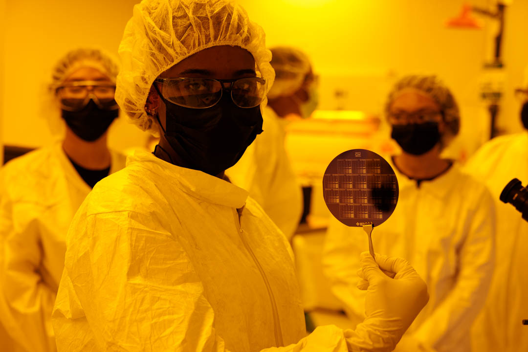
The team will produce silicon wafers comprising of hundreds of microchips, which will be distributed to the community. The goal is to provide researchers with an accessible pre-planarized chip platform suitable for integration and for benchmarking the performance of their novel devices against other devices from the community.
“This partnership is extremely important and comes at a critical time because it provides the research infrastructure needed to make advancements in the field of nanotechnology and semiconductor devices, particularly as the United States shifts its strategic focus to the reshoring of microchip production” Adam said.
This approach enables novel devices that are promising to be demonstrated in an integrated platform, which can facilitate their quick adoption into the production of new chips and ultimately into new computing applications and consumer products —“from lab to fab to market,” as she puts it.
Adam's group is using GW's nanofabrication facility, located in Science and Engineering Hall, as well as NIST's Center for Nanoscale Science and Technology to develop and test new chips. Her team integrates existing chip technology with new emerging devices called memristors to enable “neuromorphic” applications, meaning they mimic the computational power of the human brain and nervous system.
“Our group at GW is the first university partner showing successful integration of emerging devices onto this prototyping platform” Adam said.
For Adam, one exciting aspect of this project is that her GW students are working on both device fabrication and circuit design, thus developing the pipeline for the next generation of the workforce. Imtiaz Hossen, a third-year electrical engineering doctoral student working on memristor fabrication and integration, said that the project made him aware of the interdisciplinary challenges and what it takes to build semiconductor chips using new device technologies.
Lei Zhang, a fourth-year electrical engineering doctoral student working on circuit design, said the project is an important opportunity to develop professional skills. “Thanks to the resources and facilities provided by Professor Adam and GW, I have designed five chips with different technologies since I started my Ph.D. program,” Zhang said.
For Joseph Riem, a first-year doctoral student in computer engineering working on prototyping, the project is an opportunity to be part of intriguing new research. He was working as a software engineer in Chicago when he heard from Adam about joining her team, and while he hadn’t planned to go back to graduate school so soon, he was so interested in the project that he sped up his educational timeline.
“I really like the hardware aspect of engineering—designing the layers on the chip, where you keep stacking and stacking different materials and properties so you get what you want at the end. It almost seems a little mystical, but it’s very scientific,” Riem said. “You almost feel like a wizard, carving the symbols into the silicon. And eventually you get this new product that actually 'thinks' and processes information for you."


