By Kristen Mitchell
A group of local ninth and 10th grade students recently had the opportunity to explore the field of nanotechnology at the George Washington University School of Engineering and Applied Science (SEAS), learning what it means to create some of the extremely small electronic devices that keep the world running.
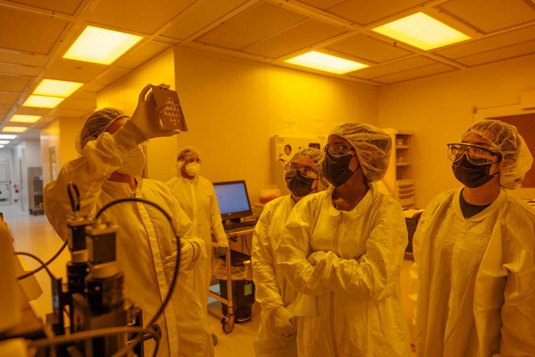
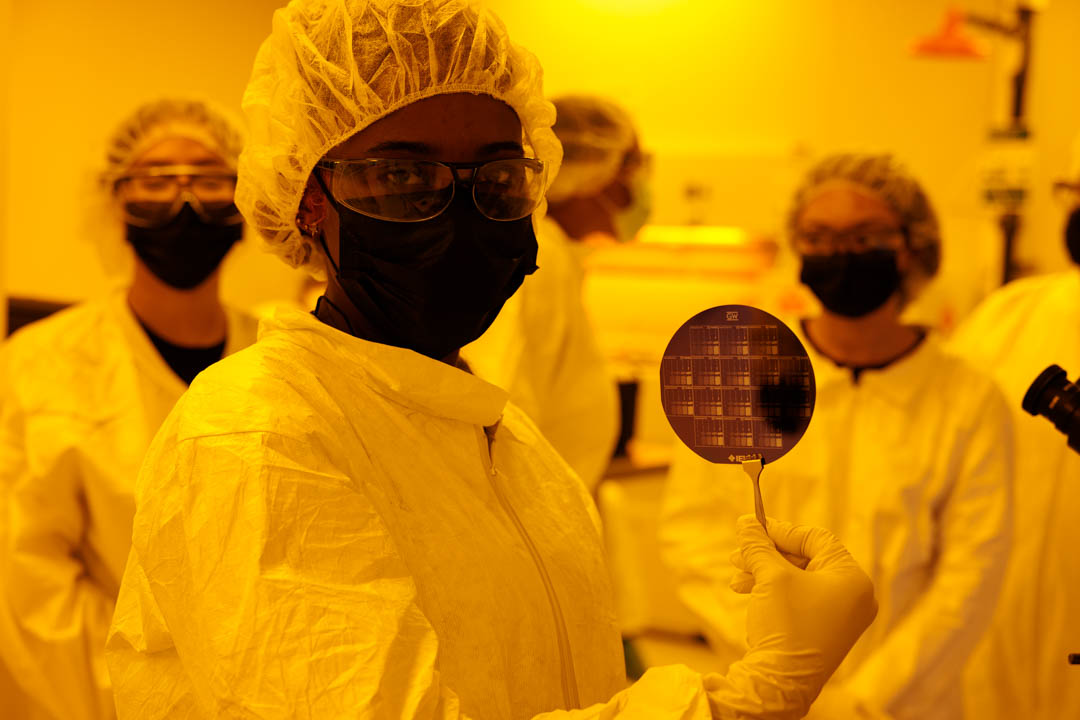
Earlier this month, Gina Adam, assistant professor in the Department of Electrical and Computer Engineering, led a two-day on-campus learning experience for students from the Girls Global Academy, a Washington, D.C. charter school with a focus on encouraging the next generation of female leaders in business and engineering. Students learned about nanoengineering and how to build electronic devices, such as resistors, transistors and memristors, using tools in the GW Nanofabrication and Imaging Center’s (GWNIC) cleanroom, a facility that maintains a very low concentration of airborne particulates and pollutants. This type of environment is necessary for building devices on the micrometer and nanometer scales, where even a stray speck of dust can disrupt the process.
Adam has been eager to put on a youth outreach program since coming to GW in 2018. Early exposure to engineering disciplines is critical to getting more women and diverse contributors in the field, she said.
“It’s very beneficial for students to understand early on what this field is and how important it is,” she said. “There's going to be an increasing demand on the job market for this trained workforce. We need to build the pipeline for future engineers, technicians and scientists in the field.”
On the first day of the outreach event, 11 students and two teacher chaperones participated in a Foggy Bottom campus tour, received an introduction to the field of nanotechnology and participated in lab safety training and virtual reality cleanroom pre-training. The virtual reality cleanroom, developed in Adam’s group by Sean Letavish, B.S. ‘22, gives users a low-pressure opportunity to become familiar with the cleanroom processes and tools.
“It allows students to learn more about these machines and how they operate without the fear of breaking them, or work with these chemicals without the fear of hurting themselves or others,” Letavish said. “Once students get to a point where they can get into a facility, they're already miles ahead of where I was when I came to GW.”
The students participated in hands-on cleanroom experiments, imaging demonstrations and electrical characterization on day two. The outreach event was supported by the Electron Devices Society of the Institute of Electrical and Electronics Engineers.
Several additional SEAS faculty and Anastas Popratiloff, director and lead research scientist for the GWNIC, were involved in organizing and ensuring the success of this learning experience. Exposure to these engineering concepts has the potential to be “transformative” for high school students as they start to think about what types of careers they could pursue in the future, Popratiloff said.
“This experience is going to stay with them because they're at this stage of human development where these kinds of opportunities make a long lasting fingerprint on their behavior,” he said. “The earlier we expose youth to these capabilities… that may change the course of their lives.”
The high school students enjoyed the learning excursion, Adam said. The GW team hopes to build on this experience and host similar outreach events in the future.
The GWNIC provides university-wide core infrastructure for academics and research, and integrates cutting-edge instrumentation and customized support services for imaging, elemental analysis, materials characterization, measurement and fabrication. The center, located in Science and Engineering Hall, opened in 2015.