
A team led by George Washington University School of Engineering and Applied Science researchers developed and demonstrated for the first time a silicon-based electro-optical modulator that is smaller, as fast as and more efficient than state-of-the-art technologies.
By adding indium tin oxide (ITO)—a transparent conductive oxide found in touchscreen displays and solar cells—to a silicon photonic chip platform, the researchers were able to create a compact device 1 micrometer in size and able to yield gigahertz-fast, or 1 billion times per second, signal modulation.
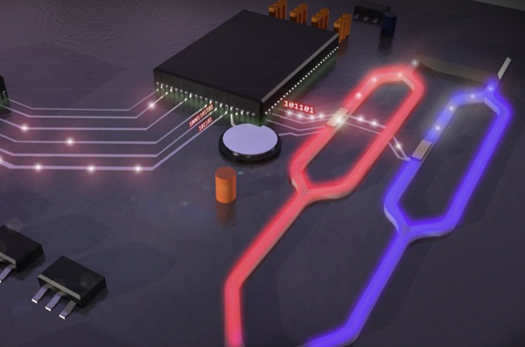
Electro-optical modulators are the workhorses of the internet. They convert electrical data from computers and smartphones to optical data streams for fiber optic networks, enabling modern data communications like video streaming.
The new invention is timely since demand for data services is growing rapidly and moving toward next generation communication networks. Taking advantage of their compact footprint, electro-optic converters can be utilized as transducers in optical computing hardware such as optical artificial neural networks that mimic the human brain and a plethora of other applications for modern-day life.
“We are delighted to have achieved this decade-long goal of demonstrating a GHz-fast ITO modulator,” said Volker Sorger, an associate professor of electrical and computer engineering. “This sets a new horizon for next-generation photonic reconfigurable devices with enhanced performance yet reduced size.”
The research team’s findings were recently published in the journal Optica.
Electro-optical modulators in use today are typically between 1 millimeter and 1 centimeter in size. Reducing their size allows increased packaging density, which is vital on a chip. While silicon often serves as the passive structure on which photonic integrated circuits are built, the light matter interaction of silicon materials induces a rather weak optical index change, requiring a larger device footprint. While resonators could be used to boost this weak electro-optical effect, they narrow devices’ optical operating range and incur high energy consumption from required heating elements.
By heterogeneously adding a thin material layer of indium tin oxide to the silicon photonic waveguide chip, Dr. Sorger’s team demonstrated an optical index change a thousand times larger than silicon. Unlike many designs based on resonators, this spectrally-broadband device is stable against temperature changes and allows a single fiber-optic cable to carry multiple wavelengths of light, increasing the amount of data that can move through a system.
This technology is covered by several patent applications and is available for licensing.